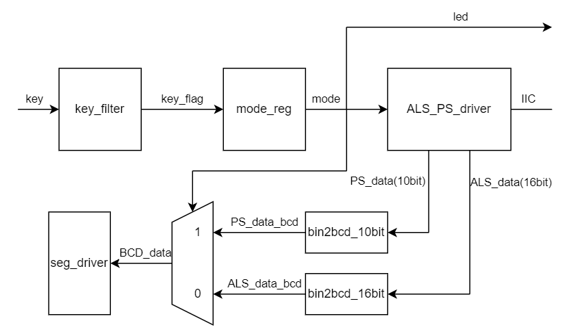
1
2
3
4
5
6
7
8
9
10
11
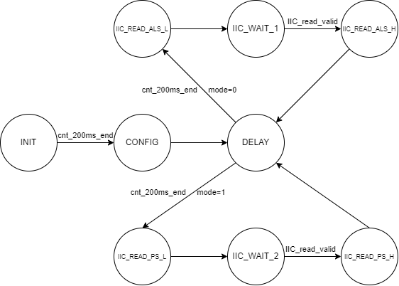
12
13
14
15
16
17
18
19
20
21
22
23
24
25
26
27
28
29
30
31
32
33
34
35
36
37
38
39
40
41
42
43
44
45
46
47
48
49
50
51
52
53
54
55
56
57
58
59
60
61
62
63
64
65
66
67
68
69
70
71
72
73
74
75
76
77
78
79
80
81
82
83
84
85
86
87
88
89
90
91
92
93
94
95
96
97
98
99
100
101
102
103
104
105
106
107
108
109
110
111
112
113
114
115
116
117
118
119
120
121
122
123
124
125
126
127
128
129
130
131
132
133
134
135
136
137
138
139
140
141
142
143
144
145
146
147
148
149
150
151
152
153
154
155
156
157
158
159
160
161
162
163
164
165
166
167
168
169
170
171
172
173
174
175
176
177
178
179
180
181
182
183
184
185
186
187
188
189
190
191
192
193
194
195
196
197
198
199
200
201
202
203
204
|
// -----------------------------------------------------------------------------
// iic驱动,支持400khz,支持地址位宽1字节、2字节,支持单字节读写
// -----------------------------------------------------------------------------
module iic_driver
#(
    // 寄存器地址宽度
    parameter ADDR_WIDTH = 2,
    // 野火开发板EEPROM设备地址为0x53,1010011,这里作为默认地址
    parameter DEV_ADDR = 7'b1010011
)
(
    input               clk,
    input               rst_n,

    // host side
    input               rd_req,
    input               wr_req,
    input   [15:0]      addr,
    input   [7:0]       wr_data,
    output reg          rd_valid,
    output reg  [7:0]   rd_data,

    // iic side
    output reg          scl,
    inout               sda
);
//-----------------------------------信号声明-----------------------------------
    // 由于写法问题,SCL频率默认400k,不支持100k和1M
    localparam SCL_FREQ = 400_000;
    wire [7:0] DEV_ADDR_W = {DEV_ADDR, 1'b0};// 7bit设备地址 + 1bit写命令(低电平)
    wire [7:0] DEV_ADDR_R = {DEV_ADDR, 1'b1};// 7bit设备地址 + 1bit读命令(高电平)
    // 状态机,一共16个状态
    reg [3:0] state, next;
    localparam IDLE    = 0,        // 空闲
               START1  = 1,        // 起始位1
               DEV_W   = 2,        // 7bit设备地址 + 1bit写命令(低电平)
               ACK1    = 3,        // 设备地址应答
               ADDR_H  = 4,        // 地址高字节
               ACK2    = 5,        // 地址高字节应答
               ADDR_L  = 6,        // 地址低字节
               ACK3    = 7,        // 地址低字节应答
               WR_DATA = 8,        // 写数据
               ACK4    = 9,        // 写数据应答
               START2  = 10,       // 起始位2
               DEV_R   = 11,       // 7bit设备地址 + 1bit读命令(高电平)
               ACK5    = 12,       // 设备地址应答
               RD_DATA = 13,       // 读数据
               NO_ACK  = 14,       // 无应答
               STOP    = 15;       // 停止位
    // 读写状态寄存,0为写,1为读
    reg is_read;
    // wr_data寄存
    reg [7:0] wr_data_r;
    // addr寄存
    reg [7:0] addr_h, addr_l;
    // 读数据寄存器
    reg [7:0] rd_data_r;
    // 应答信号寄存
    reg ack_r;
    // scl计数器,400khz则为125时钟周期,但125不能被4整除,所以选择128,产生的scl频率约为390khz
    reg [6:0] scl_cnt;
    // bit计数器
    reg [2:0] bit_cnt;
    // 内部sda
    reg sda_r;
    // sda三态门输出使能
    wire sda_oe;
    // sda三态门
    assign sda = sda_oe ? sda_r : 1'bz;
    // scl计数器满,127,即7'b1111111
    wire scl_cnt_end = &scl_cnt;
    // 1字节结束,当scl_cnt == 7'b1111111 且 bit_cnt == 3'b111时,表示1byte结束
    wire byte_end = scl_cnt_end & (&bit_cnt);
//---------------------------------输入信号寄存---------------------------------
    // 地址寄存
    always @(posedge clk, negedge rst_n) begin
        if(!rst_n)
            {addr_h, addr_l} <= 0;
        else if(state == IDLE && (rd_req | wr_req))
            {addr_h, addr_l} <= addr;
    end
    // 写数据寄存
    always @(posedge clk, negedge rst_n) begin
        if(!rst_n)
            wr_data_r <= 0;
        else if(state == IDLE & wr_req)
            wr_data_r <= wr_data;
    end
//-----------------------------------------------------------------------------
    // 读状态寄存,读优先,不在读状态即为写状态
    always @(posedge clk, negedge rst_n) begin
        if(!rst_n)
            is_read <= 1'b0;
        else if(state == IDLE)
            is_read <= rd_req;
    end
    // 状态机
    always @(posedge clk, negedge rst_n) begin
        if(!rst_n)
            state <= IDLE;
        else
            state <= next;
    end
    always @(*) begin
        case(state)
            IDLE   : next = (rd_req | wr_req) ? START1 : IDLE;
            START1 : next = scl_cnt_end ? DEV_W : START1;
            DEV_W  : next = byte_end ? ACK1 : DEV_W;
            ACK1   : next = scl_cnt_end ? (~ack_r ? (ADDR_WIDTH == 2 ? ADDR_H : ADDR_L) : IDLE) : ACK1;
            ADDR_H : next = byte_end ? ACK2 : ADDR_H;
            ACK2   : next = scl_cnt_end ? (~ack_r ? ADDR_L : IDLE) : ACK2;
            ADDR_L : next = byte_end ? ACK3 : ADDR_L;
            ACK3   : next = scl_cnt_end ? (~ack_r ? (is_read ? START2 : WR_DATA) : IDLE) : ACK3;
            WR_DATA: next = byte_end ? ACK4 : WR_DATA;
            ACK4   : next = scl_cnt_end ? (~ack_r ? STOP : IDLE) : ACK4;
            START2 : next = scl_cnt_end ? DEV_R : START2;
            DEV_R  : next = byte_end ? ACK5 : DEV_R;
            ACK5   : next = scl_cnt_end ? (~ack_r ? RD_DATA : IDLE) : ACK5;
            RD_DATA: next = byte_end ? NO_ACK : RD_DATA;
            NO_ACK : next = scl_cnt_end ? STOP : NO_ACK;
            STOP   : next = scl_cnt_end ? IDLE : STOP;
            default: next = IDLE;
        endcase
    end
    // scl计数器
    always @(posedge clk, negedge rst_n) begin
        if(!rst_n)
            scl_cnt <= 0;
        else if(state != IDLE)
            scl_cnt <= scl_cnt + 7'd1;
    end
    // bit计数器
    always @(posedge clk, negedge rst_n) begin
        if(!rst_n)
            bit_cnt <= 0;
        else if(state == DEV_W || state == ADDR_H || state == ADDR_L || state == WR_DATA || state == DEV_R || state == RD_DATA) begin
            if(scl_cnt_end)
                bit_cnt <= bit_cnt + 3'd1;
        end
    end
    // scl 每个周期持续128系统时钟周期,scl_cnt[6:5]变化规律为00-01-10-11,所以可以用于调整scl电平,保证sda在scl低电平中间进行跳转
    always @(*) begin
        case(state)
            IDLE   : scl = 1'b1;
            // 与非 1110
            // ___
            //    |_
            START1 : scl = ~(scl_cnt[6] & scl_cnt[5]);
            // 或 0111
            //   ___
            // _|
            STOP   : scl = scl_cnt[6] | scl_cnt[5];
            // 异或 0110
            //   __
            // _|  |_
            default: scl = scl_cnt[6] ^ scl_cnt[5];
        endcase
    end
    // sda_oe 在应答状态和读数据状态,允许sda输入
    assign sda_oe = ~((state == ACK1) || (state == ACK2) || (state == ACK3) || (state == ACK4) || (state == ACK5) || (state == RD_DATA));
    // sda_r
    always @(*) begin
        case(state)
            START1, START2: sda_r = ~scl_cnt[6];            // 下降沿
            DEV_W         : sda_r = DEV_ADDR_W[~bit_cnt];   // 7bit设备地址 + 1bit写命令
            ADDR_H        : sda_r = addr_h[~bit_cnt];       // 地址高字节
            ADDR_L        : sda_r = addr_l[~bit_cnt];       // 地址低字节
            WR_DATA       : sda_r = wr_data_r[~bit_cnt];    // 写数据
            DEV_R         : sda_r = DEV_ADDR_R[~bit_cnt];   // 7bit设备地址 + 1bit读命令
            STOP          : sda_r = scl_cnt[6];             // 上升沿
            default       : sda_r = 1'b1;
        endcase
    end
    // 采样应答信号
    always @(posedge clk, negedge rst_n) begin
        if(!rst_n)
            ack_r <= 1'b1;
        else if((state == ACK1) || (state == ACK2) || (state == ACK3) || (state == ACK4) || (state == ACK5)) begin
            if(scl_cnt == 7'b0111111)  // 在scl高电平中间进行采样
                ack_r <= sda;
        end else
            ack_r <= 1'b1;
    end
    // 读数据
    always @(posedge clk, negedge rst_n) begin
        if(!rst_n)
            rd_data_r <= 0;
        else if(state == RD_DATA && scl_cnt == 7'b0111111)// 在scl高电平中间进行采样
            rd_data_r <= {rd_data_r[6:0], sda};
    end
    // 输出读数据
    always @(posedge clk, negedge rst_n) begin
        if(!rst_n) begin
            rd_valid <= 1'b0;
            rd_data  <= 8'h00;
        end else if(is_read && state == STOP && scl_cnt_end) begin
            rd_valid <= 1'b1;
            rd_data  <= rd_data_r;
        end else begin
            rd_valid <= 1'b0;
            rd_data  <= 8'h00;
        end
    end
endmodule
|